
13917 Deviar Dr
Centreville, VA 20120
dstew@cpuville.com


The addition operation takes a binary input and produces a unique corresponding binary output. To make a logic circuit that performs addition, we need to combine the basic logic gates in such a way that the circuit maps a given input to a specific output, according to the addition truth table. Any time the digital circuit designer needs to map an input to a certain output, he or she can use the technique of AND-OR arrays. Circuits designed this way may not be the most efficient in terms of number of gates used, but you can always make the circuit you need. The AND-OR array method will be used again in this book to design logic to control a computer arithmetic logic unit and for the logic that interprets machine code instructions.
Recall the matrix and truth tables for binary addition:
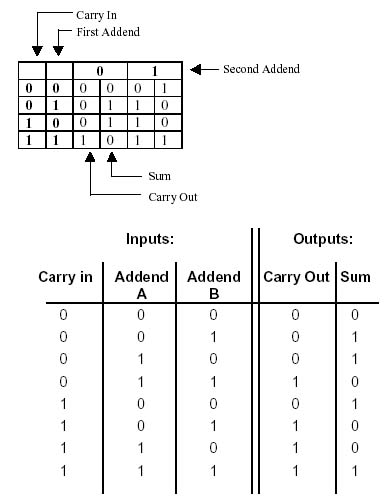
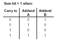
Unlike the basic logic gates, the adder will need three inputs (addends and carry in) and will have two outputs (sum and carry out). To design the adder circuit, or any combinatorial logic circuit using an AND-OR array, we start by looking at each output bit, and write down which input combinations will cause that bit to be a 1. We only have to design the circuit to output the 1, because if it does not, by default the output will be zero. From the addition truth table, we note that there are four combinations of the three input bits that will result in the sum bit being 1. These 4 combinations are 001, 010, 100, and 111. We write a list, like this:
We write the same list for the conditions that result in the Carry-out bit being a 1:
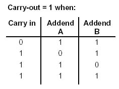
Next, we simplify the list a little. Note that bit patterns 110 and 111 both cause the carryout bit to be a 1. That is, when our circuit calculates the carry out bit, if the carry-in and addend A are both 1, it does not care what addend B is. We can substitute an X for "don't care" in the list of inputs that cause the carry-out bit to be 1:
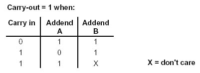
In order make an adder using AND-OR design, we think like this. For the carry-out bit, we can look at the list we made and say:
The carry-out bit will be 1 when:
carry-in is 0, AND addend A is 1, AND addend B is 1
OR
carry-in is 1, AND addend A is 0, AND addend B is 1
OR
carry-in is 1, AND addend A is 1.
You get the idea that we can use AND gates and OR gates to create a circuit that will perform this logical operation. To design an AND-OR array to perform addition we draw a diagram such as this:
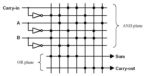
This diagram is not a schematic of a circuit, but rather a picture that shows what we want the circuit to do. The grid at top, called the AND plane, represents multiple input AND operations as vertical lines. Each dot on a line represents an input to that particular AND operation. For example, the first vertical (downgoing) line represents a 3-input AND operation that has as its inputs the inverse of the carry-in bit, the inverse of the addend A bit, and the uninverted addend B bit. More formally, it is
(NOT (carry-in)) AND (NOT (addend A)) AND (addend B)
The circuit symbol for this AND operation would be

This AND operation comes from the first line in the sum bit = 1 truth table for addition. The other vertical lines represents the other AND operations needed for the sum = 1 and carry-out = 1 tables. There are 6 three-input AND operations, and one two-input AND operation. We do not need to design AND operations for inputs that result in the sum or carry-out bit being zero, because if they are not 1 they will automatically be 0.
Below the grid for the AND operations is a grid made of two horizontal lines that end in arrows. This grid is the OR plane. Each horizontal line represents a multiple-input OR operation that has as its inputs the outputs of the operations from the AND plane above. In the diagram above, the outputs of the first four AND operations serve as inputs to a 4- input OR operation, the output of which is the Sum bit. Similarly, the last 3 AND outputs are ORed together to make the carry-out bit.
From this logical diagram we can create a circuit diagram for the one-bit adder. We need three inverters, which are already shown. We need six three-input AND gates and one two-input AND gate. You have seen that we may use two two-input AND gates to make a single three-input gate, so we will need 13 two-input AND gates total. We need three two-input OR gates to make a single four-input OR gate for the sum bit, and two more for the three-input OR for the carry-out bit, so we need 5 two-input OR gates in all.
We can reduce the gate count a little if we notice that some of the AND operations are the same, such as (NOT (carry-in)) AND (addend A). This AND operation is seen in both the second and fifth columns, labeled as 1 in the figure below, so we need only one two-input AND gate for this instead of two. The output this one gate can be sent to the inputs of both of the second AND gates to finish the operations.
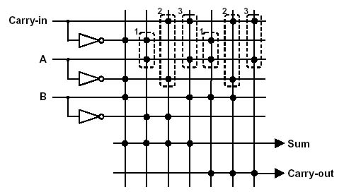
Similarly, the operation (carry-in) AND (NOT (addend A)) is in both the third and sixth columns, labeled as 2, and (carry-in) AND (addend A), labeled 3, is in the fourth and seventh column. Now we only need a total of 10 two-input AND gates for the complete adder circuit.
Here is a circuit diagram of the adder. The three AND gates that are used twice are also labeled below.
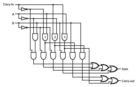
The circuit has one noticeable flaw. The inputs are each connected to several gates, meaning that the adder will appear to draw more current than a single standard input. This is easily corrected by adding a non-inverting buffer at each input. Then, the adder inputs will appear to be the same as the inputs of any other logic gate. In fact, we can use a symbol for the adder just as we would for the logic gates.
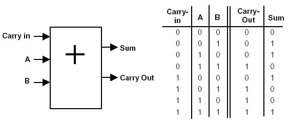
Like the other logic gate circuits, the power supply inputs are not shown, but understood to be present.
The basic adder circuit shown above is able to add only two one-bit numbers and a carry. However, these one-bit adders, like other logic circuits, are designed so that they can be connected together in networks. When combined as pictured below, we can easily make a circuit that will add two 4-bit binary numbers.
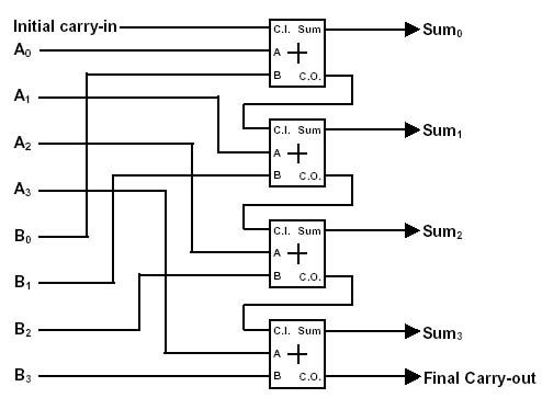
Finally, we can put all this in a box and we now have a four-bit adder.
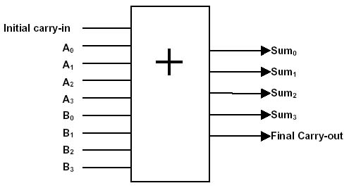
We can make an 8-bit adder from two four-bit adders, and so on to make a circuit that can add numbers of any size.
You have seen how complex circuits can be made of NAND gates. In fact, any circuit that takes a binary input and has a corresponding binary output can be made the same way. By use of AND-OR array logic we can make circuits that decode addresses and instructions.