Donn Stewart
13917 Deviar Dr
Centreville, VA 20120
dstew@cpuville.com
13917 Deviar Dr
Centreville, VA 20120
dstew@cpuville.com
Consider the following circuit:
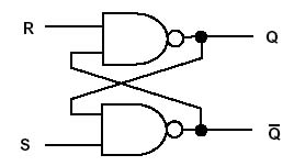
Here are two NAND gates with their outputs cross-connected to one input on each. This arrangement makes use of feedback. When R and S are 1, the circuit has two stable states: Q can be 1 and Q' 0, or Q can be 0 and Q' 1. Suppose the circuit has Q = 1. If S goes to 0, even momentarily, the circuit will flip states and Q will become 0. If S goes back to 1, Q will remain 0 (and Q' 1). The circuit "remembers" that S was 0 at some time in the past. Then, if R goes to 0, the circuit will flip back to the way it was initially, with Q = 1 and Q' = 0. This behavior is central to circuits that hold data. These circuits are used in computer memory and registers. The circuit above is called the R-S (reset-set) latch. It is the central circuit of the more complex circuits called flip-flops.
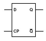
Here is a circuit called a data or D-type flip-flop:
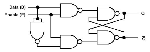
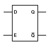
It is an RS latch with additonal NAND gates that make it simple to control. When Enable is 0, both control NAND gates will have a 1 output, and the RS latch will remain stable. When Enable = 1, Q will become equal to Data. If Data changes while Enable = 1, Q will also change. When Enable goes back to 0, the most recent value of D will remain on the Q output (and Q' will be the opposite). The D-type flip-flop has its own symbol, of course.
This flip-flop is sometimes called a transparent latch, because while Enable is high, the data outputs follow the data input. Because the latch holds the data forever while the enable input is low, it can be used to store information, for example, in a computer memory. Lots of latches plus a big decoder equals one computer memory.
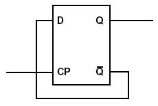
If two data-type latches are connected as below, the result is an edge-triggered latch:
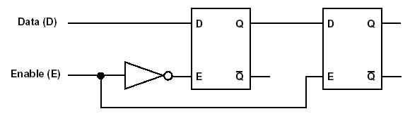
In this configuration, two transparent D-type latches are connected in tandem. The enable input, when low, causes the first flip-flop to be in the transparent state, and the second flip-flop to be locked. When Enable goes high, the second flip flop becomes transparent first, then after a brief delay the first flip-flop becomes locked. The output of the second flip-flop will show the locked output of the first. Even though the second latch is in its transparent state, the data on the output will not change, because the first latch is locked. When enable goes low again, the second flip-flop becomes locked first, then the first becomes transparent. The data output will remain unchanging, because now the second flip-flop is locked. The only time new data can be stored in the circuit, is during the brief moment when the enable input goes from low to high. This transition is referred to as a rising clock edge, and so this tandem latch configuration is called a rising edge triggered latch. The two flip-flops and inverter can be enclosed by a box, and represented by a single symbol. The Enable input of the transparent latch is replaced by the clock pulse (CP) input. The edge-triggered latch is one of the central circuits in computer design.
It allows the following:
Assume a series of pulses (voltage going from 0 to 5V) is coming in to the CP input. The Q output will be switching values every other clock pulse. This divides the clock frequency by two. A chain of these acts as a binary counter.
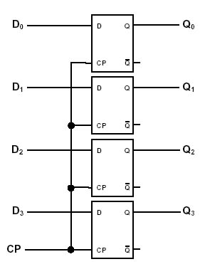
The most important use of the edge triggered flip-flop is in the data register. The characteristic of loading data only at the rising edge of the clock pulse is critical in creating the computer machine cycle, as we will see. A register is simply a collection of edge triggered flip-flops. Here is a four-bit register:
The edge-triggered flip-flop register is crucial for the computer machine cycle. The machine cycle can be characterized by the following (very much abbreviated) diagram.
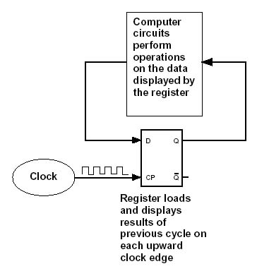
The computer clock provides a continuous stream of pulses to the computer processor. With each upward swing of the voltage on the clock output, the register loads whatever values are present on its inputs. As soon as the data is loaded it appears on the outputs, and stays there steady throughout the rest of the clock cycle. The data on the register outputs is used as input for the computer circuits that carry out the operations desired. For example, the accumulator register data output may be directed by a multiplexor to one of the inputs of the ALU, where it serves as an addend. The result of the addition appears on the ALU outputs, which can be directed by multiplexors to the inputs of the same accumulator register. The result waits at the inputs of the register for the next upward swing of voltage on the CP register input, sometimes called the write input (WR). When this occurs, the ALU result is loaded into the register and displayed on the outputs. The value held in the register from the previous cycle is overwritten and discarded, having served its purpose. The cycle is repeated endlessly, the data following paths dictated the program instructions, which control the various multiplexors and registers. If the accumulator had used transparent latches, the ALU result would feed through the register, to the ALU, back to the register and through again to the computer circuits in an uncontrolled loop. The edge-triggered register ensures that the result is written in an instant, and then the inputs close, allowing the computer to perform its operations in an orderly and stable way.