Donn Stewart
13917 Deviar Dr
Centreville, VA 20120
dstew@cpuville.com
13917 Deviar Dr
Centreville, VA 20120
dstew@cpuville.com
For many years I have had the hobby of making computer processors. I do this for fun. It is a hobby with an educational dimension since I put details of the processors on my public website for others to see and comment on. My most recent processor is described here:
CPUville 8-bit processorIt was my intention with that project to make a processor that could take the place of the 8-bit Z80 processor I use in my Single-board Z80 computer kit. The 8-bit processor I designed is NOT a Z80 clone; far from it. The Z80 has over 200 instructions in its instruction set; the 8-bit processor I made has exactly 28 (or 29 if you count the no-operation instruction NOP). The 8-bit processor has the same address, data and control lines as the Z80, so it can operate the same system (the memory and input/output ports) but its architecture (internal registers, instruction format and machine language) are completely different. The 8-bit processor is a pure accumulator-memory machine, meaning it has only one register, the accumulator, and all operations that involve actions on data (moving data and arithmetic/logic operations) use this register. For operations involving two operands, such as addition, one operand will be in the accumulator, the other will be taken from memory, or contained in the instruction itself (an immediate value).
The processor works well. As a “Turing complete” machine it can run all the algorithms any other classical computer can. A demonstration program of a calculation of the value of pi to 7 decimal digits using numerical integration shows its capability.
However, programming this machine is difficult. There are three main difficulties. The first is that it lacks the extra registers of most other processors you might be familiar with, so there is lots of extra work putting and retrieving values from memory. Indexing is the second problem, but this can be solved by placing an instruction in RAM and modifying the instruction address operand directly. But the more serious third problem is recursion.
Recursion is the ability of a code segment to call itself as a subroutine. This process is facilitated by the processor stack, a data structure controlled by a special register, the stack pointer. The 8-bit processor I made lacks a hardware stack pointer, so any kind of subroutine call or (limited) recursion requires a stack-like structure to be created in software. This can be done of course, but the cost is substantial. I found this out when I tried to create a compiler for this processor.
The language I chose to compile was variant of the B language, which is the subject of some “Write Your Own Compiler” projects I saw. As I worked, I had to cope with the lack of a hardware stack in the target machine. The lack of registers other than the accumulator made the resulting object code very long. Typically, one B language statement would generate 25 lines of assembly language, and between 50 to 100 bytes of machine code. The executable code for a simple program to print out a series of prime numbers ended up being 7.5 kilobytes long. If I had written it directly in assembly language it would have been less than 1 kilobyte.
So I gave up on the compiler project. What was needed was a more capable machine. I toyed with the idea of making a new processor, but the thought of wire-wrapping a new hardware processor gave me pause. So I decided to try making a processor in an FPGA (field programmable gate array).
The FPGA is the modern descendant of the 1980’s era PALs (programmable array logic) and GALs (generic array logic) that I was familiar with. The PALs and GALs are ICs that have circuits that can be programmed to implement several dozen logic gates. One GAL I used in my Z80 computer for the memory control logic saved me from using 7 discrete logic ICs, and a trio of GALs in the 8-bit processor for the next-state logic saved me about 30 ICs, or one entire circuit board.
Modern FPGAs can be programmed to implement many thousands of logic gates and flip-flops. Complicated circuits, such as computer processors, digital signal processors, and graphics display processors can be built with them. For hobbyists and students, there are low cost development boards that have an FPGA and some support circuits on them that make using them pretty simple.
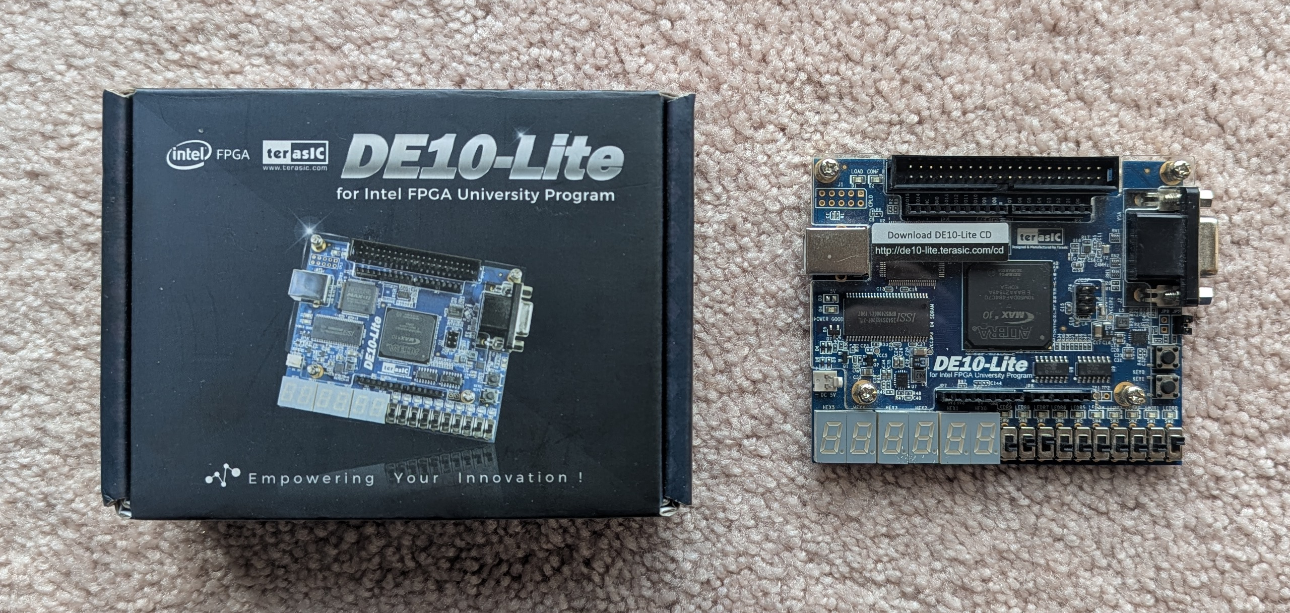
I saw that there were many used FPGA development boards for sale on eBay, typically by students that had used them for a university course but had no further use for them. I ended up buying a used Terasic DE-10 Lite board for about $95 on eBay. This board is built around an Altera Max 10 FPGA device. The board was used in the Intel FPGA University Program, and being sponsored by Intel I figured there would be good documentation, tutorials and software available to program and use this device. That turned out to be true.
There was quite a lot to learn to use the FPGA. The device is programmed using a hardware-description language (HDL). This language is a little like a high-level programming language, except instead of describing a procedure or algorithm, it describes a circuit. There are two commonly used HDLs, VHDL and Verilog (or its newer version, System Verilog). Like a computer language, you write the code in plain text, and compile it with the appropriate software. The output is a configuration file that is sent to the FPGA to implement the design.
I chose Verilog, and began looking at the tutorials using this HDL to configure FPGAs. For someone who is familiar with programming languages HDL can be a little confusing at first. With HDL you are describing hardware, and not a process. The blocks you create in the HDL do not describe events or functions that take place in a sequence, like they do in a programming languages, but rather circuit elements. If you want events to happen in a sequence in your design, you have to create a clock signal and create sequential logic circuits. Otherwise, if you describe a lot of combinational logic circuits, everything happens at the same time. There are lots of YouTubes by HDL mavens that help you understand this.
The essential element of circuits in Verilog is the module. A module has ports for input and output, and some kind of internal structure. The internal structure of a module is made of combinational logic blocks and sequential logic blocks. Combinational logic is described in always @* blocks (or always_comb blocks in System Verilog), and sequential logic is described in always @(posedge clock)-style blocks (or always_ff blocks in System Verilog). Sequential logic blocks can also use negedge, and other clock-type signals. There are other block types but these are the main ones I used.
Once you have described your modules, you can instantiate your modules inside other modules, and connect the modules to signals you have created in a higher module. There is a hierarchy with the topmost module being your final circuit. In my case the topmost module had the CPU connections to the DE-10 board defined, and the actual CPU module was instantiated in this connections module. The ports of the CPU module are the address bus, data bus, and control signals read, write, memory request, and input-output request, the same as can be found on a Z80. Inputs to the CPU module are the system reset line, and the computer clock. The CPU module instantiates the other modules needed in the CPU, such as the program counter and arithmetic-logic unit, described below. For debugging I also brought out the state register value to a CPU module port so I could use the LEDs on the DE-10 board to follow the states as the processor ran. When the CPU inside the FPGA was finished, the DE-10 could take the place of the Z80 in the computer system.
Here is a description of the path I took from being a total FPGA noob to creating a working processor. I did not start out making the CPU modules. Instead, I followed the tutorials of the Intel FPGA University Course which is about making simple circuits such as counters, adders, multiplexers and similar that require a small number of logic gates. I could compile the Verilog code for these circuits using Quartus software (the Lite version is free). The configuration files produced could be sent to the FPGA on the DE-10 board over a USB connection using a programmer tool provided with Quartus (the USB connection also powers the DE-10). The tutorial circuits make use of the DE-10 switches, buttons and LEDs for inputs and outputs.
As I gained confidence in writing Verilog I began to think seriously about the FPGA CPU project. The goal of this project was to make a processor that would operate the system on the Z80 computer board, taking the place of the Z80. I intended to use the general-purpose input-output (GPIO) connections on the DE-10 to connect to the Z80 system bus, and use the Z80 system’s memory and ports, like the 8-bit processor does. There were enough GPIO signals on the DE-10 board (36) to operate the system. These GPIO signals, along with +3.3V, +5V and ground connections, were available on a 40-pin header on the DE-10.
To electrically connect the DE-10 to the Z80 system board I had to overcome two problems. First, the DE-10 signals were +3.3V, and the Z80 system signals were TTL-level (+5V). Second, the Z80 system signals had to mapped to the correct pins on the DE-10. So an adapter of some type was needed.
I designed a simple adapter that I thought would do the trick on the same KiCad software that I have often used to design my circuits. The adapter was small, so I just ordered some prototype PCBs from OSH Park instead of making a wire-wrap adapter board.
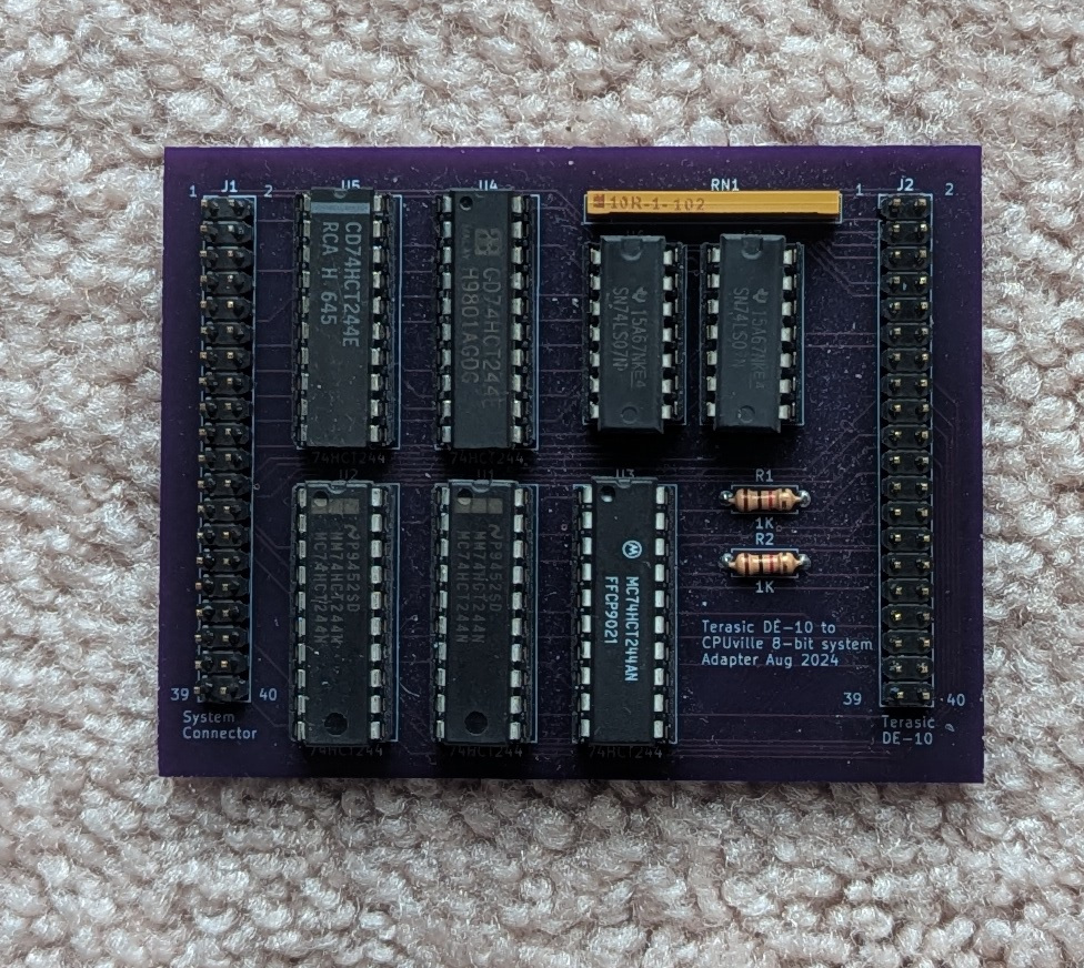
Besides mapping the signals, the adapter uses an open-collector buffer (74LS07) to change the high voltage of signals coming from the Z80 system to the DE-10 from +5V to +3.3V. The low voltage for signals for both systems was 0V, and both systems shared a common ground. For the +3.3V signals coming from the DE-10 to the Z80 system, regular non-inverting buffers (74LS244) were adequate, since the minimum voltage needed to produce a +5V output from these buffers was +2.0V. I connected the DE-10 to the adapter with a two-plug 40-conductor ribbon cable, and the adapter to the Z80 system board (with the bus display attached) with a three-plug cable.
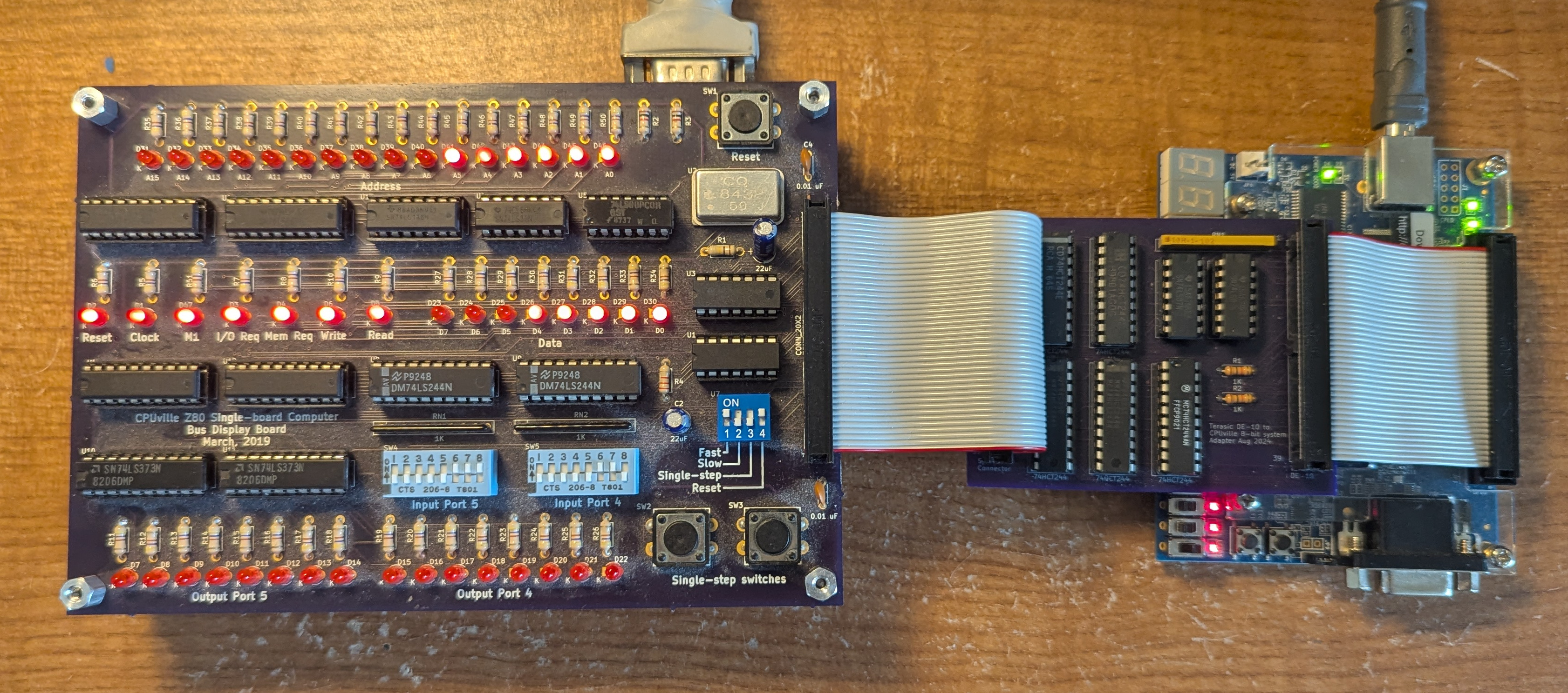
After a few tests I was confident the system and DE-10 were communicating properly, and I began to work on Verilog modules for the new processor. Here is a description of the new processor architecture.
The Z80 system I made (the Single-board Z80 computer) has an 8-bit, bidirectional data bus and a 16-bit address bus, so that would be the starting point. Therefore, the new FPGA processor would be an 8-bit processor with a 64KB memory space. Instead of a single register, I decided to start with 4 registers, A, B, C, and D. My plan was also to use these registers in pairs, AB and CD, for operations requiring 16-bit operands such as indexing. I decided on variable length instructions, from one to four bytes, so I would have four 8-bit registers to contain the current instruction, IR-A, IR-B, IR-C, and IR-D. I also planned a 16-bit Address register, which would send an address to the system address bus.
The Z80 system has a bi-directional data bus, which for me was the most difficult thing to code in Verilog. After scouring the net for examples, and after much trial and error I found I could use this module:
module bidirec (oe, inp, outp, bidir);

input wire oe;
input logic [7:0] inp;
output logic [7:0] outp;
inout wire [7:0] bidir;

assign bidir = !oe ? inp : 8'bZ ;

always_comb outp = bidir;

endmodule
This module warrants a description. The bidirectional data bus wires are connected to the bidir port. These will be certain GPIO pins, and they have to be declared as inout. This allows them to take a hi-Z value, as is typical of any hardware that is bidirectional. The output enable signal oe tells the module what the data direction is. This signal is used in the assign bidir = !oe ? inp : 8'bZ ; statement. This statement uses the Verilog a ? b : c construct to select the value to be assigned to the bidir port. That is, if a = 1 the value is b, otherwise c. In my CPU, I used a direction signal Dir for managing the bidirectional port. The Dir signal would have an opposite polarity from the oe signal in the bidirec module. That is, if Dir was zero, that meant that the DE-10 was putting data onto the system bus, and if 1 was reading data from the data bus. This Dir signal controlled a ‘244 buffer in the adapter. When Dir was zero this enabled the buffer to output data to the data bus. I used the inverse expression !oe to make the bidirec module function match the meaning of the Dir signal.
The module takes data in at the inp port, and puts it on the bus if !oe = 1 (that is, when Dir = 0). If !oe = 0 the bus connection is placed in the hi-Z state. The always_comb block statement makes the module output outp equal to whatever is on the bus. So, when the module is in the output direction, outp will be equal to inp. When the module is in the input direction, since the bus wires of the port are made hi-Z, outp will be whatever data some other hardware is putting on the bus. (Note that inp and outp refer to the bidirectional port itself, and NOT to the data bus). I tested the bidirectional port on the DE-10 by making an FPGA design that would read a byte from the system serial port (terminal keyboard) and echo it out to the same port (to the terminal display). This worked properly.
The other processor modules were much more straightforward. The main modules of the data path were the program counter, stack pointer, and the arithmetic-logic unit (ALU). The registers for data and the instruction did not require distinct modules, they are just declared in Verilog statements. The program counter would have a 16-bit output and be incremented after each byte of an instruction was read from memory, and could have its value replaced by another 16-bit value for jump instructions. The stack pointer was a 16-bit value that could be incremented, decremented, and replaced. The ALU would be an essentially combinational circuit that would perform add, add with carry, subtract, subtract with borrow, logical AND, OR, XOR and NOT. The ALU would also produce output bits for a zero result, a negative result (minus), and a carry-out. These bit signals would be saved in registers in the CPU as flags for use in conditional instructions, and as a carry-in for add with carry and subtract with borrow. Here are the program counter, stack pointer, and ALU modules:
module program_counter (clk, rst_l, action, data_in, data_out);

	input wire clk, rst_l;
	input logic [1:0] action;
	input logic [15:0] data_in;
	output logic [15:0] data_out;

	logic [15:0] temp;

	always_comb begin
		case (action)
		2: temp = data_in;
		1: temp = data_out + 16'h0001;
		0: temp = data_out;
		default: temp = data_out;
		endcase
	end

	always_ff @(posedge clk) begin
		if (!rst_l) data_out <= 16'h0000;
		else data_out <= temp;
	end

endmodule
module stack_pointer (clk, rst_l, action, data_in, data_out);

	input wire clk, rst_l;
	input logic [1:0] action;
	input logic [15:0] data_in;
	output logic [15:0] data_out;

	logic [15:0] temp;

	always_comb begin
		case (action)
		3: temp = data_in;
		2: temp = data_out - 16'h0001;
		1: temp = data_out + 16'h0001;
		0: temp = data_out;
		endcase
	end

	always_ff @(posedge clk) begin
		if (!rst_l) begin
		data_out <= 16'h0000;
		end
		else data_out <= temp;
	end

endmodule
module ALU (op, a, b, ci, co, z, m, out);

	input logic [2:0] op;
	input logic [7:0] a, b;
	input wire ci;
	output wire co, m;
	output logic z;
	output logic [7:0] out;

	logic [8:0] temp;

	assign co = temp [8];
	assign m = out [7];

	always_latch begin
	case (op)
	0: begin
	   temp = a + b;
	   out = temp [7:0];
	   if (out == 0) z = 1; else z = 0;
	   end
	1: begin
	   temp = a + b + ci;
	   out = temp [7:0];
	   if (out == 0) z = 1; else z = 0;
	   end
	2: begin
	   temp = a - b;
	   out = temp [7:0];
	   if (out == 0) z = 1; else z = 0;
	   end
	3: begin
	   temp = a - b - ci;
	   out = temp [7:0];
	   if (out == 0) z = 1; else z = 0;
	   end
	4: begin
	   out = a & b;
	   if (out == 0) z = 1; else z = 0;
	   end
	5: begin
	   out = a | b;
	   if (out == 0) z = 1; else z = 0;
	   end
	6: begin
	   out = a ^ b;
	   if (out == 0) z = 1; else z = 0;
	   end
	7: begin
	   out = ~a;
	   if (out == 0) z = 1; else z = 0;
	   end

	endcase

   end

endmodule
Verilog mavens (especially those who write processors) will certainly get a laugh at my beginners code, but it works. I find Verilog to be a fairly forgiving language.
With the basic architecture decided on I created the instruction set for the processor. I just thought of the instructions I wanted, and made a list of the instructions that would fit the architecture. Here is the final instruction set:
miniCPU instruction set

Mnemonic      Opcode=IR_A Opcode Length  IR_B     IR_C     IR_D
                   (dec)  (hex)  (bytes)
NOP        		0	00	1
ADD reg,reg		1	01	2	0000aabb
ADC reg,reg		2	02	2	0000aabb
SUB reg,reg		3	03	2	0000aabb
SBB reg,reg		4	04	2	0000aabb
AND reg,reg		5	05	2	0000aabb
OR reg,reg    		6	06	2	0000aabb
XOR reg,reg		7	07	2	0000aabb
NOT reg			8	08	2	000000aa
MOV reg,reg		9	09	2	0000aabb
MOV reg,value		10	0A	3	000000aa  value
MOV reg,[mem]		11	0B	4	000000aa  addr_lo  addr_hi
MOV [mem],reg		12	0C	4	000000aa  addr_lo  addr_hi
PUSH reg    		13	0D	2	000000aa
POP reg			14	0E	2	000000aa
CALL         		15	0F	3	addr_lo   addr_hi
RET        		16	10	1
JP address   		17	11	3	addr_lo   addr_hi
JPC address		18	12	3	addr_lo   addr_hi
JPNC address		19	13	3	addr_lo   addr_hi
JPM address		20	14	3	addr_lo   addr_hi
JPNM address		21	15	3	addr_lo   addr_hi
JPZ address		22	16	3	addr_lo   addr_hi
JPNZ address		23	17	3	addr_lo   adder_hi
SCF         		24	18	1
CCF        		25	19	1
IN reg,[port]		26	1A	3	000000aa  port
OUT [port],reg		27	1B	3	000000aa  port
MOV SP, address		28	1C	3	addr_lo   adder_hi
INC reg			29	1D	2	000000aa
DEC reg			30	1E	2	000000aa
MOV reg, [reg pair]	31	1F	2	00000aap
MOV [reg pair], reg	32	20	2	00000aap
INC reg pair		33	21	2	0000000p
DEC reg pair		34	22	2	0000000p
The meaning of most of the instructions is evident from its mnemonic. Some that might be a little obscure are SCF, CCF, the conditional jumps, and ADC and SBB. SCF and CCF are set carry flag and clear carry flag. The conditional jumps are jump-if-carry, jump-if-not-carry, jump-if-minus, jump-if-not-minus, jump-if-zero, and jump-if-not-zero. ADC is add with carry, and SBB is subtract with borrow.
The second byte of many instructions has the registers to be used, in the bit locations designated by aa, or aabb in the case of instructions using two registers. So, for ADD A,B the first byte of the instruction would be the opcode 01h, and the second byte would be 0000 0001b, with the A register designated by 00b, and the B register by 01b. Instructions using register pairs are shown with a p bit to designate a register pair, with 0 for the AB pair, and 1 for the CD pair. Other operands are 8-bit values, or 16-bit addresses. Note the inclusion of instructions using the stack, CALL, RET, PUSH, and POP, and MOV SP which sets the stack pointer to a new value.
With the architecture, some basic hardware modules and the instruction set in hand I now set about making the processor function. This means making a state machine.
The state machine is the central core of any computer processor. In fact, you could even say that a computer processor IS a state machine, with some bells and whistles added that make it perform data manipulations. The processor state machine has a number stored in it, the current state. At the next clock edge, the processor performs actions dictated by the current state number, such as writing values to certain registers, or changing a control signal. At the same clock edge, the current state is replaced by the next state, which is a number produced by the combinational next-state circuit. The next-state circuit takes as input the current instruction opcode, the current state, and system flags such as carry or zero, and gives the next state as an output. When the current state is replaced by the next-state, the new current state dictates the actions the processor will perform at the next clock edge, and will be replaced by the next next-state, and so on forever. The current state is forced to zero by the reset signal (along with the program counter and stack pointer). State zero is the beginning of the instruction fetch cycle, so after reset the processor will fetch the instruction in location zero of memory. The CPU instantiates the program counter, stack pointer, ALU, next-state function, and the bidirectional data bus connection modules. The rest of the CPU module is a list of states and the actions to be performed at each state in an always_ff (posedge clock) block as a long case statement (a Verilog statement similar to the same thing in C, but implemented as a multiplexer in hardware). The next-state circuit is a separate module of combinational type. The CPU and next-state modules are fairly long so I put links here to the text files:
FPGA processor CPU main moduleThe next state module is written as a case statement with each state subdivided into next-states that depend on the current instruction opcode and in some cases on the processor flags. Near the end of the next-state module is the list of states that produce a next state = 0. These are the last states of each instruction action, and state 0 is the beginning of a new instruction fetch.
For completeness I add here the uppermost module which describes the connections between the DE-10 GPIO pins and the processor module:
//CPU to operate CPUville 8-bit system

module MiniCPU_synth (GPIO, LEDR, CLOCK_50);

	inout wire [35:0] GPIO;
	output [9:0] LEDR;
	input wire CLOCK_50;  //For dual boot function to add design to configuration flash memory

	wire Reset;
	wire [15:0] Address;
	wire Clock;
	wire Read;
	wire Write;
	wire IO_Req;
	wire Mem_Req;
	wire [7:0] State;
	wire Dir;	//zero causes the bidirectional port to output data to system bus

	wire Clock_top;

	assign LEDR [7:0] = State;
	assign GPIO [25:10] = Address;
	assign GPIO [28] = IO_Req;
	assign GPIO [26] = Mem_Req;
	assign GPIO [32] = Read;
	assign GPIO [33] = Dir;
	assign GPIO [34] = Write;
	assign Clock = GPIO [30];
	assign Reset = GPIO [35];

	dual_boot U0 (.clk_clk (CLOCK_50), .reset_reset_n (1'b1));
	miniCPU U1 (Reset, Address, GPIO [7:0], Clock_top, Read, Write, IO_Req, Mem_Req, State, Dir);

	always_comb Clock_top = ~Clock;

endmodule
For some reason the DE-10 did not like the clock input from the Z80 system board unless I fed it through an inverter on the DE-10. Thus the always_comb Clock_top = ~Clock; statement. The dual-boot module you see instantiated here is for putting the design into the DE-10 flash configuration memory, which will load the design into the FPGA when you power up the board.
One of the fun things about making a processor in an FPGA is the ease of changing the design. You can add instructions by adding the actions to the CPU module, and the next-state information to the next-state module. Also, in a hardware design, if the next-state function is hard wired in logic, you often re-use states to save hardware gates, but the FPGA is very large and you can just add states as you need them, similar to processor microcode in a ROM. So, my original IC hardware 8-bit processor had a total of 21 states, but the FPGA processor has 103 states (numbered 0 to 102).
I got the point where I could run short snippets of machine code on the FPGA processor by hand-assembling the bytes for a short program and burning them into a 2K ROM and placing this in the ROM socket on the Z80 computer system board (without the Z80 of course). I could test instructions for memory and port reading and writing, and the arithmetic instructions. However, it soon became apparent that debugging the Verilog code for the CPU using only the LEDs on the DE-10 and the Z80 system board was too difficult. Fortunately, there is software that will simulate your design, and you can look at all the values in all the modules one clock tick at a time to see where you are going wrong. This is Questa, or Questa Sim. To use Questa Sim one needs to write a special Verilog module called a testbench, and make this the top module in your design. Then you instantiate the module you want to test (often called the design under test, DUT) inside the testbench, which provides signals to stimulate your module, and you can run the simulation and look at every value and every wire. It took me a while to figure out how Questa worked, but soon I was having great fun using this software. The strangest bugs would eventually yield to deep probing, and things to which I said “that’s impossible!” eventually were solved. You can even read a binary file into synthetic memory in Questa Sim, so I could run code on the processor in Questa Sim like I could on the Z80 system board. I could also create input-output ports in the testbench and use those as well. I am very grateful to whoever produced Questa Sim. Again, for completeness here is a link to the testbench module for the processor:
FPGA processor testbench moduleThe testbench module includes functions to open a binary file and read it into a memory structure in the testbench. The testbench also creates reset and clock signals for input into the CPU module. The testbench module also instantiates a bidirec2 module, which is identical to the bidirec module instantiated in the CPU except its direction (response to the Dir signal) is the opposite of the bidirec module. This allows the testbench to communicate with the CPU over a bidirectional data bus.
I have for many years used the excellent program TASM, and the newer TASM32 as an assembler for my processor projects. This is not the Borland Turbo Assembler for x86 architecture, but the Telemark Assembler authored by Tom Anderson, available at ticalc.org. One writes a table file with your bespoke assembly language and opcodes, and the assembler reads this file and assembles the binary file output for you. Just a great program for those who design processors. Here is my TASM table file for the FPGA processor and the Hello, World! program:
;Test assembly language file

			.org	0000h

			call	initialize_port
			call write_string
halt:			jp	halt

initialize_port:	mov 	a,04eh		;1 stop bit, no parity, 8-bit char, 16x baud
			out 	[3],a			;write to control port
			mov 	a,037h			;enable receive and transmit
			out 	[3],a			;write to control port
			ret

;Subroutine to write a zero-terminated string to serial output
;Get address of string from string_pointer
;No error checking
write_string:	mov	d,[string_pointer]	;lo byte of pointer
			mov	c,[string_pointer + 1]	;hi byte of pointer
ws_loop:		in 	a,[3]			;read status
			mov	b,01h
			and 	a,b			;check TxRDY bit
			jpz 	ws_loop		;loop if not set
			mov	a,[cd]		;get char of string
			push	a			;temp storage
			mov	b,0
			or 	a,b			;check if 0
			pop	a			;get char back
			jpz	quit			;if char 0 quit
			out 	[2],a			;char not zero, output
			inc	cd			;point to next char in string
			jp 	ws_loop		;start over
quit:			ret

string:		.db	"Hello, world!",0dh,0ah,0
string_pointer:	.dw	string

			.end
There comes a point in any processor project when instead of reaching for the logic probe (or running Questa Sim) when you hit a bug you begin to look more carefully at your code. I recall that point in this project, when something wasn’t working in my Hello, World! program. I had the CPU in Questa Sim to see what the problem was, and I saw that I had made an error in the assembly language. I have since written some more code, and it seems the processor is working correctly. Next step will be writing a monitor program for the system so I can load programs over the serial link, and eventually maybe a compiler.
--Donn Stewart, October 2025