Donn Stewart
13917 Deviar Dr
Centreville, VA 20120
dstew@cpuville.com
13917 Deviar Dr
Centreville, VA 20120
dstew@cpuville.com
It is a simple matter to make a NAND gate out of transistors and a resistor:
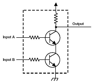
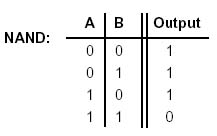
The resistors on the inputs limit the base-emitter current to just enough to turn the transistors on. It is important to understand that the inputs are not connected to the output, they only determine whether the output is connected to +5V or 0 V. You can see that this circuit performs the NAND operation. If both transistors are on (both inputs +5V or 1) the output will be connected to ground (be at 0V or 0). If either transistor is off, the output is connected through the resistor to +5V. Here is the circuit behavior presented as a truth table:
The circuit I have shown above is sometimes called transistor-resistor logic, because of the resistor between the output and the +5V power supply. In most commonly used NAND circuits, there are extra transistors take the place of this resistor. This improves the performance of the circuit and makes it especially easy to connect to other digital circuits. These improved logic circuits are called transistor-transistor logic (TTL).
Now that you understand the NAND circuit, we will forever bury the details of it inside a closed box, hiding it from view. Once we have this circuit in hand, we are concerned only with how to form larger functional units using NAND gates as the basic building block. If the gates are well designed, as in TTL, they can be hooked up one to another in essentially unlimited networks. We do not need to know the details of their construction in order to use them.
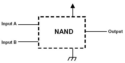
Here, all the details are hidden. The last transformation is to replace the box and the word "NAND" with a certain shape. This will be the schematic symbol for the NAND circuit.
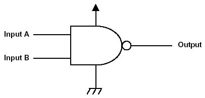
Since all digital circuits circuits have the same +5V and 0V power supply connections, we can eliminate them from the symbol. However, never forget that they are present.
Since the output of the circuit can sink or source much more current than the inputs use, the output of one NAND gate can be connected to the input of others in endless chains and infinite combinations. There are a few limitations. First, a single NAND input does requires a little current. A NAND output can supply (or sink) a large, but not infinite, current. Because of this, the number of inputs that a single NAND output can be connected to is limited. In practice, an output can control or drive about 10 inputs. This is called the "fan out" of the gate. This is not much of a restriction, since most of the circuits we will make will have fan-outs of only a few gates.
The other limitation is that outputs can never be connected together. Outputs can be connected to inputs, and inputs to inputs, but never outputs to outputs. This is because outputs can source or sink a large current, and if two connected outputs are opposite (a one and a zero) there is in effect a short circuit which would damage the components. In addition, the logic level of the connected outputs would not be defined, that is, it would have some value between one (5V) and zero (0 V) determined by the resistances in the connected gates.
We will now build the basic logic circuits NOT, AND, OR and XOR from NAND gates. Each logic circuit is accompanied by its truth table, as we introduced earlier. The simplest is the NOT gate, or inverter.
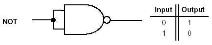
This gate is made by connecting the two inputs of a NAND gate together. Now, both inputs of the gate will always be the same, either 0 or 1. Remember the truth table of the NAND gate:
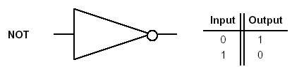
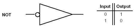
Note that when both inputs A and B are the same, the output is the opposite. By connecting both inputs together we force both inputs of the NAND gate to be both 0 or both 1, and the NOT gate is born. The NOT gate, or inverter, has its own symbol, which we will use from now on. Like the other logic gate diagrams the power supply connections are not shown, since they are understood to be there always.
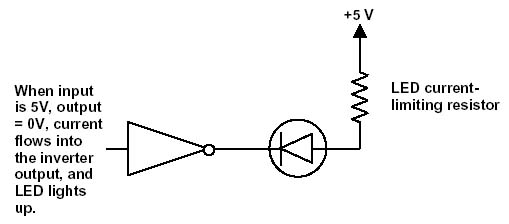
Here is a circuit diagram using a NOT gate as an LED driver. The NOT gate acts as a current sink for the LED when the NOT gate input is 1.
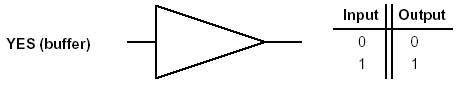
The NOT gate is also called an inverting buffer, which stresses its ability to amplify. If we hook two NOT gates together we will now have a YES gate or non-inverting buffer.
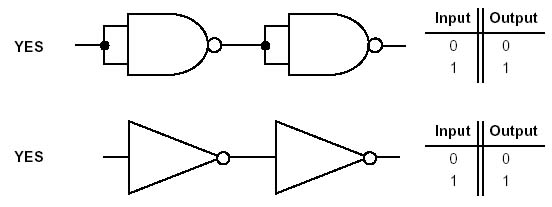
The YES gate has its own symbol
Note the only difference between the NOT and YES symbols is the little circle at the tip of the triangle. Sometimes, in logic circuit diagrams, the circle alone is used as a symbol for the NOT (inversion) operation. Since inverting the input of the YES gate has the same effect as inverting the output, an inverting buffer symbol could also be drawn as
I will try to avoid the use of the inverter symbol at inputs, but sometimes it greatly simplifies complex logic circuit diagrams.
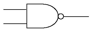
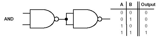
Now we come to the logic gates for the AND, OR and XOR operations. The AND operation can be made by simply inverting the output of a NAND gate.
This is the same as
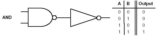
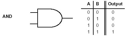
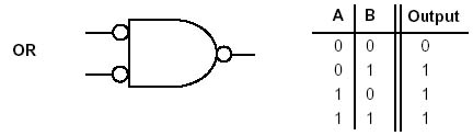
The AND gate symbol is the NAND gate without the inverting circle at the output
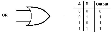
The OR gate is a little more complicated. Using NAND gates it is made this way.
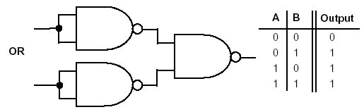
The OR gate is the NAND gate with the inputs inverted.
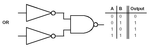
Using the circle symbols for inverting the inputs is another way to show the OR gate.
The OR gate has its own symbol.
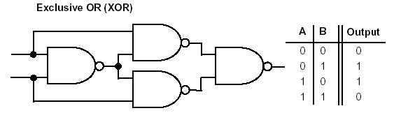
The XOR gate is built from four NAND gates.
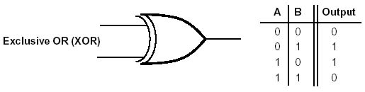
The XOR symbol is
The AND, OR and XOR gates all have complementary gates with inverted outputs. We know about the NAND gate, the complement of the AND gate. Here are the NOR and XNOR gates made with NAND gates. They are the same as the OR and XOR gates except the output is inverted.
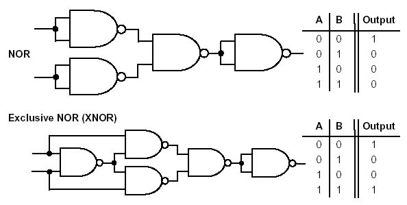
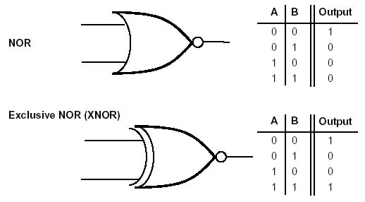
Note the additional NAND gate inverter at the output. The NOR and XNOR gates can also be symbolized using the small circle added to the NOR and XNOR schematic symbols to signify inversion of the outputs.
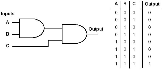
This completes the list of basic logic gates with one or two inputs, and one output. The next step up is to make gates with three inputs and one output. For our purposes, these are the three-input AND and OR gates. These multi-input gates can be made from the standard two-input gates. Here is a three-input AND gate, with its corresponding truth table:
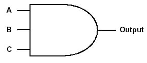
The three-input AND gate can be drawn using a single symbol.
The three-input OR gate can be made in the same way.
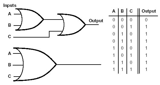
It is possible to make AND and OR gates with any number of inputs by combining two-input gates as shown above.
This completes the description of the basic logic gates. These gates can be combined to make the larger circuits needed to make a computer processor. These larger circuits are multiplexors (data selectors), registers, the adder, and the logic that controls the computer.