Donn Stewart
13917 Deviar Dr
Centreville, VA 20120
dstew@cpuville.com
13917 Deviar Dr
Centreville, VA 20120
dstew@cpuville.com
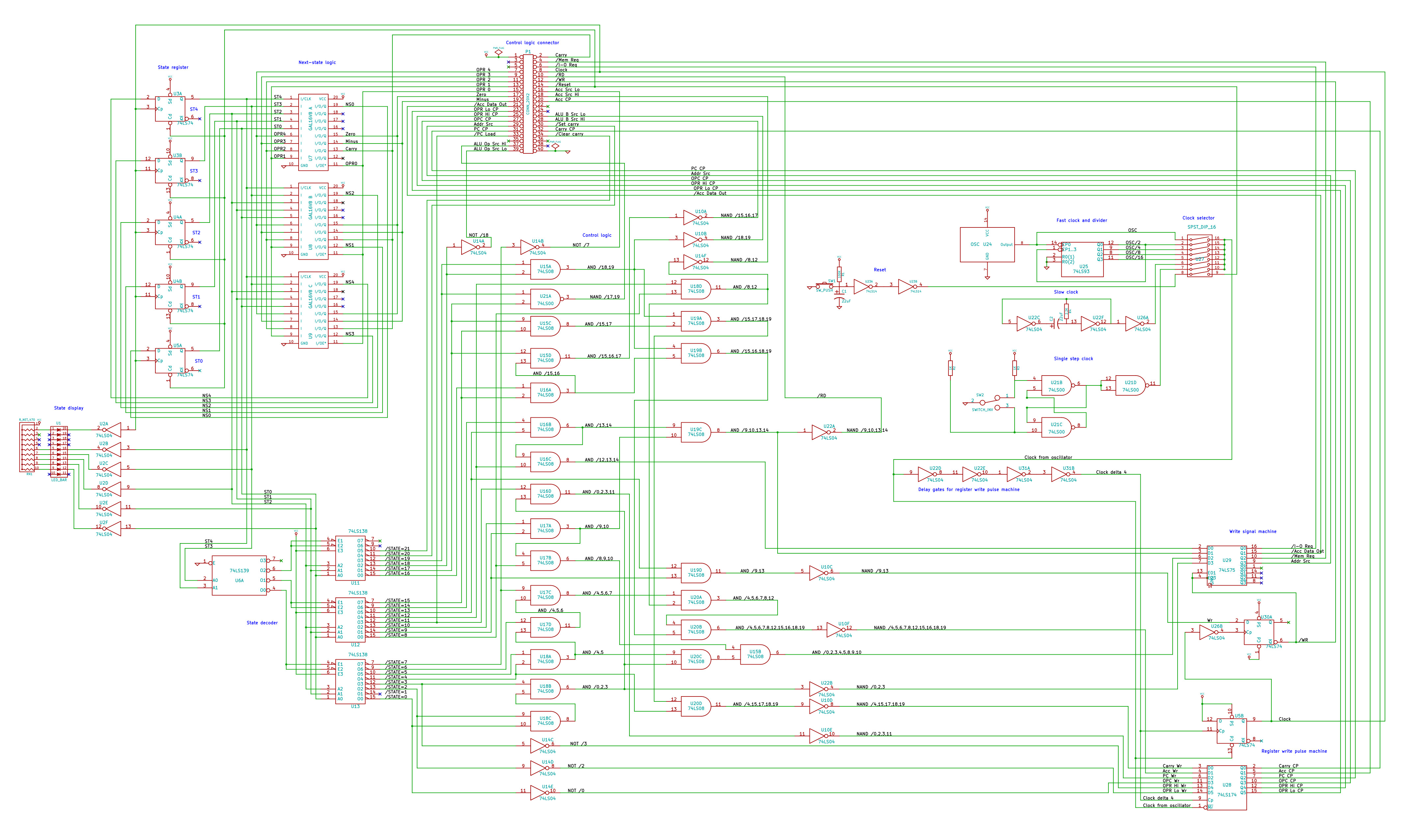
The control logic produces the signals that control the multiplexors and registers in the data path, and the system control signals memory request, input/output request, read and write. It produces these signals in response to the current state, which is a 5-bit number held in the state register. The state is determined by the current instruction, system flags, and the previous state (or the reset signal for state 0 when the computer is starting). The state machine is discussed on the finite state details page.
The current state is the input for a decoder that produces an active-low signal for that state. This active-low signal is input into a logic circuit that sets the multiplexor controls, register write signals, and the system control signals. Here is the logic for that circuit, in a table form:
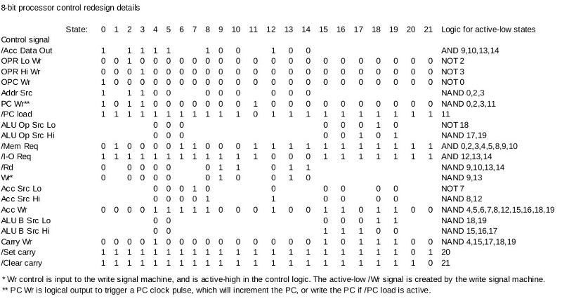
The table has a 1 or 0 in each column when a state needs that particular control to have that particular output. If a state does not care about the control, it is left blank. The state decoder produces active-low outputs, and the logic equations on the right reflect this. Each equation should produce the pattern of 1s and 0s in the row beside it as the logic goes through its various state sequences, as controlled by the finite state logic.
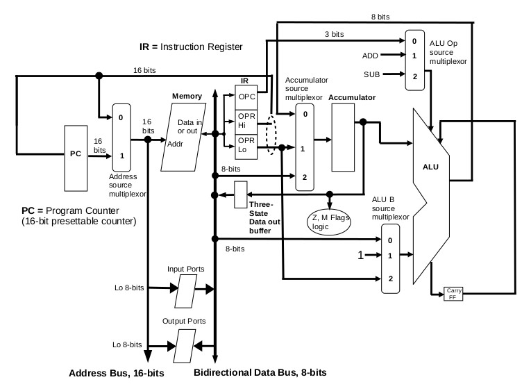
The signal names should be easy to understand if one references the data path diagram for the whole computer. For example, the signal "/Acc data out" is an active-low signal (that is the meaning of the "/") that when asserted (is low) opens the accumulator data-out buffer, putting accumulator contents onto the data bus. Signals designated as "Wr" are inputs to a special register that creates the write pulses for the various registers in the data path. For example, the "OPR Lo Wr" signal creates the clock pulse that writes data into the lowest byte of the instruction register. Signals with "Src" in their names serve as addresses for source multiplexors. For example, "ALU Op Src Lo" is the low bit of a two-bit address that selects the source of the ALU operation. "/Mem Req" and "/I-O Req" are the active low system control signals for requesting memory or an input/output port. "/Rd" is the system read control, and "Wr" is the control logic input to the write signal machine that generates the proper timing for a memory or input/output write operation. The "/Set carry" and "/Clear carry" are special signals that do just what they say, though inputs to the carry flip-flop.
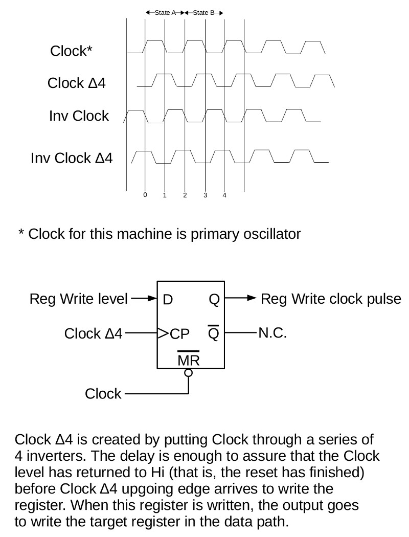
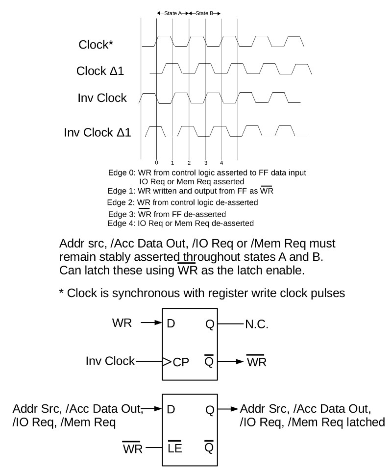
The details of the logic circuit that produces the control signals, the register clock pulse machine, and the write signal machine, can be seen in the control board schematic.
8-bit processor links: