Donn Stewart
13917 Deviar Dr
Centreville, VA 20120
dstew@cpuville.com
13917 Deviar Dr
Centreville, VA 20120
dstew@cpuville.com
The finite-state machine for the 8-bit processor generates a sequence of states, one for each clock cycle, that is specific to each machine code instruction. To do this, the output of the state register (the current state) is input to a logic circuit, along with the current instruction and the processor flags. The output of this logic circuit is the next state.
For example, the state sequence for the instruction STM (store accumulator to memory) is 0, 1, 2, 3, 9, 10. The first state, state 0, is placed in the state register by the next state logic at the end of the previous instruction's state sequence if the computer is running, or by the RESET signal if the computer is being started. State 0 is the "opcode fetch" state. In state 0, the control logic sets the system control and data path multiplexor controls to read a byte from memory at the current program counter location, and then store this byte in the opcode register by generating a write pulse for this register at the upgoing edge of the clock cycle. The program counter is also incremented. While the control logic is generating these signals, the next-state logic is generating the next-state output. In the case of state 0, the next state will always be 1, no matter what the opcode is. At the end of the clock cycle, at the upgoing edge, the next-state (1) will be written into the state register, to become the current state. State 1 is the "instruction interpretation" state, which is used to allow the next-state logic to produce the appropriate next-state for whatever instruction has been fetched. In the case of the STM instruction, the next-state will be 2, which is "fetch operand low" state, to get the low-order byte of the storage address from memory. This is followed by state 3, which is the "fetch operand high" state, to fetch the high order byte of the address. States 9 and 10 operate the "memory write signal machine" to write the accumulator to memory with the proper signal timing. Details of how the control signals are generated from the current state are found on the control signals details page. The logic used to generate the next-state from the current state, opcode and flags inputs, is discussed below.
There is a general technique for combinatorial logic called the AND-OR array technique. Briefly, each bit of the inputs, and its inverse, is made available to be combined by the AND operation (also called logical multiplication), with any other bit of the inputs. The outputs of these multi-input AND operations are combined by the OR operation (also called logical addition) for each bit of the output. The AND operations are called the "product terms", and the whole technique is sometimes called "sum of products". With this technique, any input vector (group of input bits) can be mapped to any output vector. It may not be the most efficient method, since one is not using the XOR operation, but it always works.
These sum-of-products logic arrays can be made with individual AND and OR gate ICs. There are also available circuits which have programmable AND-OR arrays, called GALs (for generic array logic) that can be used to implement the logic. I have used GALs to make the next-state logic for my control board.
To design the logic, one looks at all the input conditions under which a given output bit will be 1, and creates an AND equation for each of those conditions, and ORs them together to create the output bit. I have 22 states in my logic, numbered from 0 to 21, so I have 5 bits for the state input to the next-state logic. My instruction set has 30 instructions, so I also have 5 bits of instruction input to the next state logic. Then, I have the 3 one-bit flag inputs. In all, there are 13 bits of input to the next state logic. There are 5 bits of output, which we will take one bit at a time.
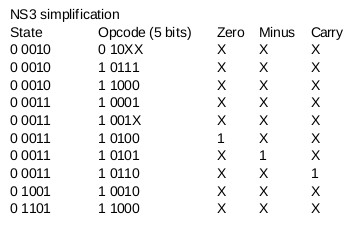
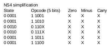
For example, we ask "when does output bit 0 need to be 1"? First we identify the states with a 1 in the bit 0 locations. These are the odd states, 1, 3, 5, etc. So, what are the inputs that need to produce an output next-state of 1? We can see from the state sequences, that if the current state is 0, no matter what the instruction or flags are, the next state will be 1. Here is a spreadsheet of the inputs to the next-state logic that will produce a 1 in the output bit NS0:
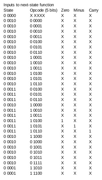
An "X" in the table means "don't care". So, the first line can be read as "NS0 will be 1 when the current state is 0, no matter what the opcode or flags are". The second line can be read as "NS0 will be 1 when the current state is 2 and the opcode is 0, no matter what the flags are." A careful observer will note that the table can be simplified, since there are some input bits that can be replaced with a "don't care". For example, lines 4 and 5 are the same, except for bit 0 of the opcode, which can be either 1 or 0. So, we can combine these two lines, and replace the opcode bit 0 with a "don't care". This can be done with many lines in the table. Here is the next-state 0 bit table simplified:
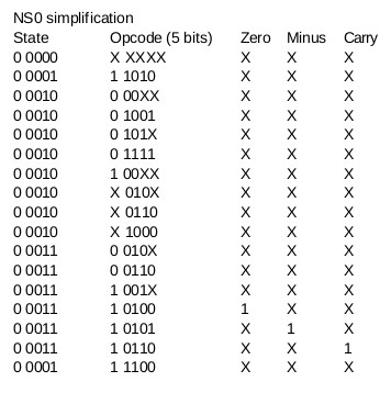
The product term for the first line, "if the current state is 0, no matter what the instruction or flags are" is (NOT state bit 4) AND (NOT state bit 3) AND (NOT state bit 2) AND (NOT state bit 1) AND (NOT state bit 0). If we shorten this a little, so that the NOT operation is replaced by the / symbol, and the AND operation is replaced by the * symbol (logical multiplication), and the input state bits are labeled S4 to S0, the equation can be written:
Next-state 0 bit = NS0 = /S4 * /S3 * /S2 * /S1 * /S0
The second line could be written:
NS0 = /S4 * /S3 * /S2 * /S1 * S0 * OP4 * OP3 * /OP2 * OP1 * /OP0
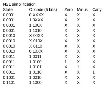
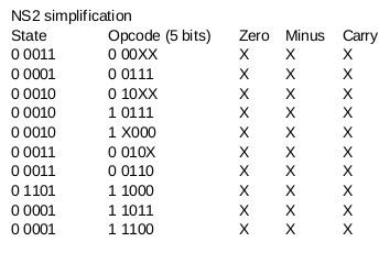
A product term can be written for each line in the table. All these product terms can be logically summed (ORed together) to produce the final logic circuit for the NS0 bit. We can also write tables for next state bits 1 to 4:
I decided to use 16V8 GALs to implement the next-state logic function. The 16V8 can have a maximum of 16 input bits, and each output bit can be the result of an OR operation of a maximum of 8 product terms. Output bits can be fed back into the array. I used three of the GAL's output cells to combine the results of the 17 product terms, and using feedback, a fourth cell to OR together those outputs for the final result. I would need 3 16V8 GALs for the whole next-state function.
I have been using a MiniPro TL866CS programmer for the EPROMs I use, and it will program the GALs as well. The programmer takes a fuse map file in the JEDEC format, which is a text file that describes the "fuses" in the GAL to write, that link the input bits together with the AND operation, and how these are combined for the output OR operations. The JEDEC file is a text file, and can be generated by hand, but there are programs that will generate a JEDEC file from logic equations. I have used the galasm program. Here is the input file for the first of the three GALs:
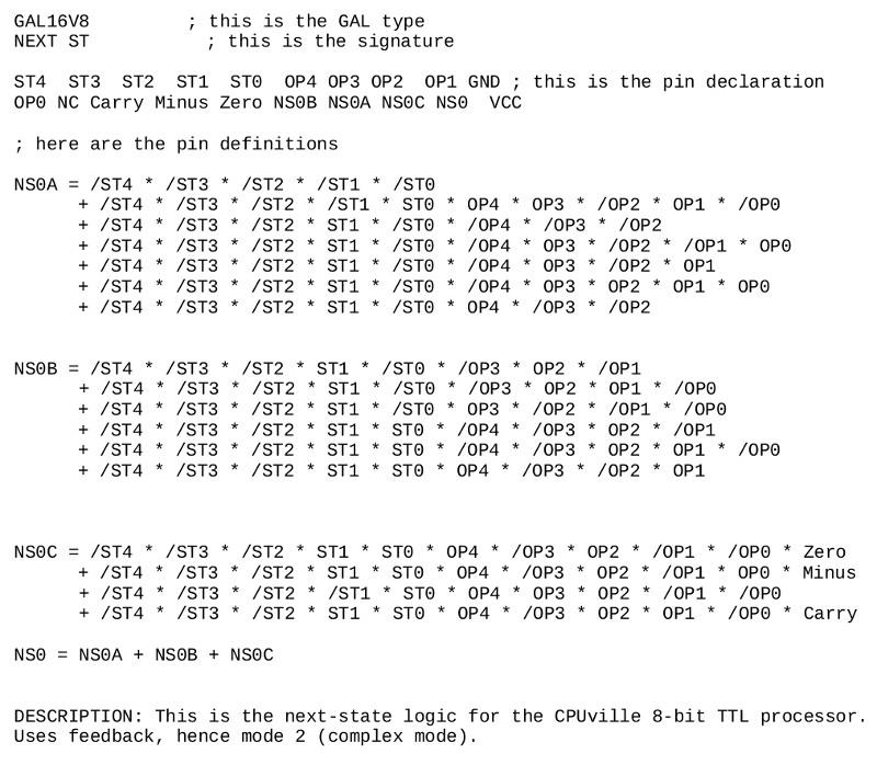
The source files for the other two GALs are similar, the equations taken from the rows in the simplified logic tables. The next-state output from the GALs is routed to the data input of the state register, and at the upgoing edge of the system clock, the next-state is written into the state register to become the current state.
8-bit processor links: