Donn Stewart
13917 Deviar Dr
Centreville, VA 20120
dstew@cpuville.com
13917 Deviar Dr
Centreville, VA 20120
dstew@cpuville.com
With the concept in hand, I now had to consider the design. I wanted to make the processor as simple as possible, that is, with a minimum of hardware, to have the best chance of success. This meant an accumulator-memory design, that is, there would be a single 8-bit data register in the processor, the accumulator, not the many registers of the Z80. The arithmetic-logic unit (ALU) would then be 8-bits wide (a simplification over the original CPUville TTL design, which had a 12-bit ALU). An appropriate instruction format would be variable, with some instructions having an opcode (8-bits) and an address (16-bits), some an opcode and an 8-bit operand, and some just an opcode. So, the instruction register would have to have space for the largest instruction, 24-bits total. With a 16-bit address space like the Z80, the program counter would need to be 16-bits. Overall, the processor would need only three registers in the data path: the program counter (16-bits), the instruction register (24-bits), and the accumulator (8-bits). There would also be a 1-bit register (a flip-flop) to hold the carry-out from the previous arithmetic operation. Here is an image of the data path:
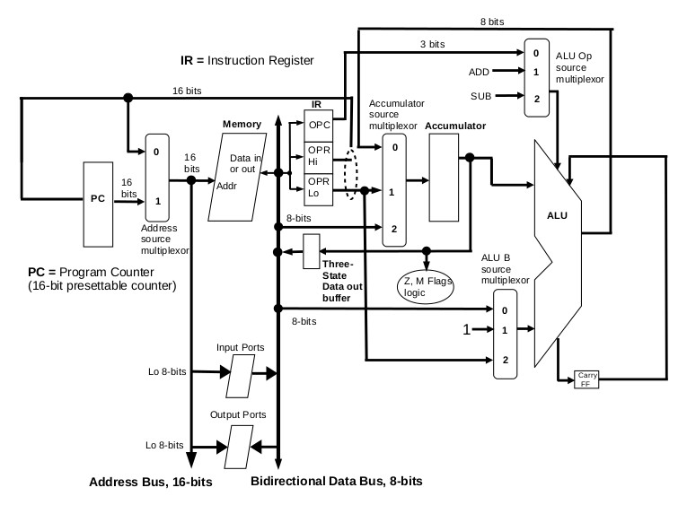
Arithmetic/logical operations would take one operand from the accumulator, and the other from either the instruction itself (immediate) or from the memory, with the memory location contained in the instruction. I also wanted to have a "one" to input to the ALU, to allow for the very useful increment and decrement instructions. The result of an ALU operation would be placed into the accumulator. I eliminated the data register that was present in the original design, it was not necessary.
The data path design influences (really limits) the instruction set. With such a simple data path, the instruction set would also be simple. For example, if you examine the data path, you find there is no way to send an address to the memory, except by having the address in the instruction. That means the instruction set will not use (or, to be more positive, does not need) any memory indirect addressing instructions, that is, instructions that use a pointer variable in RAM. This is a handicap, but it is still possible to do indirect addressing, by putting whole instructions in RAM, and then one may alter the target address of the instruction. There just won't be any instructions in the instruction set for it. But despite this and other limitations, the data path still allows for a decent instruction set:
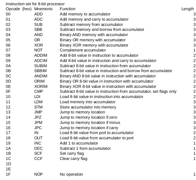
There are some unused opcodes in the instruction set, in case I think of new instructions I want to use. At present, opcodes 1D and 1E perform NOPs. I am only using the lower 5 bits of the opcode byte, so I could add many more operations, but with the current data path, I can't think of any more to add.
Like my original processor, the 8-bit processor would be built on 3 boards: an ALU, the data path (without the ALU), and the control logic. This plan served me well before, since each board has approximately the same complexity (about 30 ICs on each), and the ALU and control logic can be tested independently before being connected into the processor. The memory and input/output ports would reside on the Z80 computer system boards, which were already made and in operation. I would add a register display that connected to the data path board, mainly for hardware debugging. I would again use the wire-wrap prototyping technique, and use 74LS series TTL integrated circuits. I cannibalized my original processor, and reused the sockets, boards, and many of the ICs for the new 8-bit processor.
With my original processor, I used hand-drawn schematics that were difficult for others to follow, so with this project I decided to be more formal, and use computer-aided design for the schematics. This has the advantage that if I wanted to created printed circuit boards for this processor, it would be easy to do. I have placed images of the schematics for each part of the processor on the website, the links are on the schematics page. Another advantage of using computer-aided design is when it comes to construction, I can generate a netlist for each board. The netlist is a printout of all the "nets" in the circuit, each net being a group of pins that are wired together. This improves reliability during construction, and allows consistent use of two-level wire-wrap sockets, since each pin should have no more than two connections on it. I used Kicad for the schematics.
8-bit processor links: