Donn Stewart
13917 Deviar Dr
Centreville, VA 20120
dstew@cpuville.com
13917 Deviar Dr
Centreville, VA 20120
dstew@cpuville.com
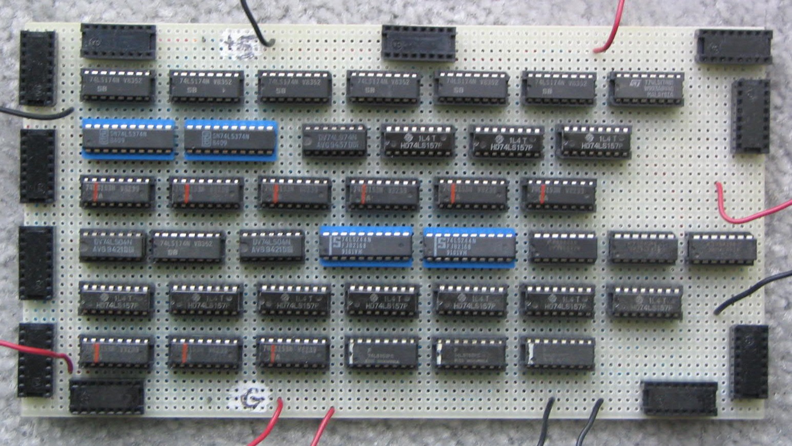
This board, which can be considered the processor main board, contains the multiplexors and data registers shown in the computer diagram seen below, and described more completely in design. The memory and the ALU are on separate boards.
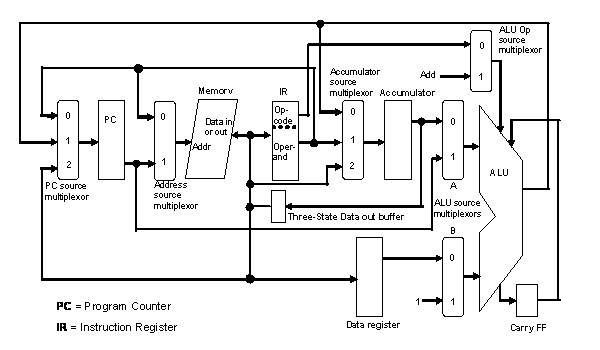
As mentioned in Design I added 4 bits to the accumulator in order to move full instruction words between input and memory, or ROM and RAM. The additional upper 4 bits of the accumulator come directly from the memory, bypassing the accumulator source multiplexor (not shown in the diagram). Whenever the accumulator is written (in arithmetic-logical instructions and accumulator loads), the upper 4 bits will therefore be from the most recently accessed memory location. Only the 12 low-order bits of the accumulator output are passed to ALU source multiplexor A. The full 16 bits of the accumulator are passed to the memory, however. Similarly, the low-order 12 bits of memory data are passed to the Data register, the PC source multiplexor input 2, and the accumulator multiplexor input 2, but the full 16 bits are passed to the instruction register (I.R.). The upper 4 bits of the I.R. are passed to the ALU operation source multiplexor, and the lower 12 bits to the accumulator source multiplexor input 1.
Some sharp visitors have noticed that the Data register does not appear to be necessary. They are correct. I was concerned that the cycle-time might not allow for data from the memory to pass through the ALU adders in time, since the adders are slowed up by having the carries "ripple" though. However, at a clock speed of 1 MHz, there is enough time for this, and I could have eliminated the Data register fetch state. But, if I try to run the computer at 4 MHz, the Data register, and its accompanying fetch state, would be necessary. I have never tried to run it that fast, though.
Also on this board, but not diagrammed, is the logic for the zero condition calculation, which is just a 16-bit NOR of the the accumulator bits. Another feature is a memory write circuit. Since the RAM is written by the level of the memory write control line, and not the edge, I used a flip-flop and an inverted system clock to create the proper timing. There are two memory write states used as seen in Control. The two states and the memory write circuit make sure that the data is held long enough, and that the memory write signal is dropped before the data changes.
One final "extra" was needed. It is imperative that all the registers are written at the same time by a clock edge in order for the computer to work. However, the logic circuits that determine if a register is to be written produce only a logic level, and they finish at different times because there are varying numbers of gates in the logic paths. The solution was to have a single register collect the write signals, and then at the same time on the same clock edge send them to their respective register write inputs. The register write inputs would see an upgoing clock edge if the logic had produced a 1, and no edge if it had produced a 0. An time-offset clock signal then resets the register after a short delay, and all the signals return to zero. This is important because if a register is to be written on two consecutive cycles, the register write signal must go back to zero in order for the next signal to produce an edge. I used a chain of several inverters to create the delay.
This board could not be tested apart from the Control, Memory and ALU boards, but since these other boards could be tested thoroughly, the debugging of the main board was pretty simple.
Links to Original CPU pages: